Difference between revisions of "HONEY Getting Started"
| Line 48: | Line 48: | ||
[[File:honey_noerc.JPG | right| thumb | <center> This is a Generic No ERC directive -- it tells Altium that this net isn't used. </center>]] | [[File:honey_noerc.JPG | right| thumb | <center> This is a Generic No ERC directive -- it tells Altium that this net isn't used. </center>]] | ||
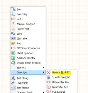
| − | [[File:placeNoerc.JPG | | + | [[File:placeNoerc.JPG | left| thumb | <center> This places one of the Generic No ERC's for nets you don't use. </center>]] |
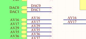
| − | [[File:usecase_nets.JPG | | + | [[File:usecase_nets.JPG | left| thumb | <center> Even though the wires don't touch -- these two are electrically connected! You can just use the name to "teleport" the connection. </center>]] |
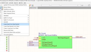
[[File:makesheetsymbol.JPG | right| thumb | <center> Here's an example of a new Sheet Symbol, and the button you use to make into an actual schematic sheet. </center>]] | [[File:makesheetsymbol.JPG | right| thumb | <center> Here's an example of a new Sheet Symbol, and the button you use to make into an actual schematic sheet. </center>]] | ||
| + | |||
===Using the TopSheet=== | ===Using the TopSheet=== | ||
The TopSheet, as mentioned, is where all of your subschematics some together and connect on a high level. Below, we'll go through some of the ways this happens. <br/> | The TopSheet, as mentioned, is where all of your subschematics some together and connect on a high level. Below, we'll go through some of the ways this happens. <br/> | ||
Revision as of 01:30, 14 August 2017
|
This is a guide Welcome! This article is intended to guide you through an SSI process. While its authors have made efforts to make it useful, if you have questions, please ask the authors on Slack. They will be able to both help you and improve this resource for future SSI-ers. This article was written by Kirill Safin ( |
|---|
| {{{header}}} | |
|---|---|
| Part of the HONEY Architecture series & the HABEES series | |
| General | |
| HONEY Standards • Venom Breakout • Fang Breakout • Board Naming | |
| Core Software | |
| STINGR | |
| Core Avionics | |
| The Count | |
| Core Power | |
| Biscuit | |
| Core Peripherals | |
| Cobra • Viper • ProtoBee | |
| Core Radio | |
| Macaw | |
| Test & Prototype | |
| QueenBee | |
| Guides | |
| Making a HONEY Board • Using STINGR • Using QueenBee • Making a Prototype | |
| V • E |
Ready to make a HONEY-compliant PCB for the HONEY Flight Stack? You've come to the right place.
This page provides specific steps and some guidance about how to get started making a HONEY-compliant PCB. Just follow along, and, if you get stuck, feel free to DM any relevant HABEES members on Slack!
Preparation
Before you design a board for the HONEY flight stack, ask yourself these questions. Answering them is useful to determine how you want to approach making a HONEY board, and whether its time to make one.
- Do you have a very specific design in mind already?
- Have you laid it out/drawn it on a schematic level, or at least discussed the EE with other HABEES members?
- Have you tested or flown your design, or a subset of your design, on a ProtoBee or Cobra?
- Have you secured the blessing/approval of the HABEES Lead? (as of writing, 8/13/17, this is Kirill Safin).
- Have you secured funding & approval from the Balloons Team?
If you answered all of those questions with YES then you are 100% ready.
If you didn't answer 2 or 3 with YES, then that's still OK! Projects are always a work in progress, and your design and thoughts will evolve with time, and as you work on the project. Prototyping and trying something before making a HONEY board is a good way to verify your design, and getting reviews from other EE members is a good way to be confident in what you're doing.
Even without that, you could make a cool board by directly making a HONEY board. All it requires is a desire to work really hard, know what you're doing, and putting in the time. If you have all that, then it's time to get started.
Getting Started
Altium
The first step to making a HONEY board is to have Altium (SSI's PCB design software of choice) set up on your computer. Altium only runs on Windows, so if you have a Mac, you'll need to install bootcamp. For instructions on how to get & set up Altium, including the SSI SVN, visit the Altium Guide on the Wiki.
Make sure you follow through all of the steps -- having everything at your disposal is crucial -- be sure specifically to add the Templates directory (found at the end of the Altium guide).
Getting Started
Got Altium set up? SWEET. Then it's time to get started. Follow the following steps.
- Make sure to update your SVN directory to the latest revision, to make sure you're up to date on the libraries & files.
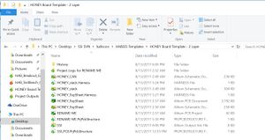
- Once you have done that, navigate to balloons -> HABEES Templates. In there, you will find a folder called HONEY Board Template - 2 Layer. DO NOT, UNDER ANY CIRCUMSTANCES, OPEN THIS PROJECT AND BEGIN WORKING. This folder is intended as a template to get you started on a HONEY board, but it can't provide that for everyone if you accidentally override it. SO, with that said -- right click and copy the folder. Then, go back to the balloons directory (one directory up). This directory has a bunch of folders, which are all balloons PCBs. Paste the template folder into here.
- Find the folder you just pasted in the balloons directory, and rename it to something meaningful. Generally, HABEES Convention for project folders is "HAB_THING_GENX". So, start it with "HAB_", decide what exactly your thingy is gonna be (i.e, MOTORDRIVER, SENSORSUITE, SOLARCHARGER, etc), and what iteration it is (are you the first to make this kind of thing? Is it upgrading a former version of the thing?), and use that to finish the folder name.
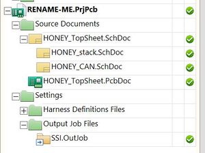
- Go inside the folder -- there's a file called RENAME_ME.PrjPcb. Rename this to whatever you want to call your project -- ideally the exact same as your folder name.
- Once you've done that, double click it to open the project in Altium (or, alternatively, open altium, click "OPEN", and navigate to this file".
- Altium will rename/recoordinate all the files, and you'll be ready to go.
Understanding the Template
Once you have the project open, there's a number of things to see and do. You need to be familiar with HONEY to really get started, so if you aren't already, head over to the HONEY page and read up. Otherwise, the following will explain what's going on:
- The HONEY Template uses multi-sheet design. This means your schematics are separated into several schematic sheets, each with a discrete purpose. That means, you can put your motor driver stuff in one, sensors in another, Teensy in another, etc. It keeps each schematic nice, clean, and focused.
- For all multi-sheet designs, there's a "top sheet" that links them all together. You'll notice there's a HONEY_TopSheet in your project. If you double click this, you'll see that this is the sheet that links everything together.
- There are two other sheets in the template.
- One is HONEY_stack.SchDoc. This takes the HONEY stack connectors -- IE power bus, data bus, CAN bus -- and breaks them out into power nets and signal nets for you to use. You generally don't need to modify this, because it'll break absolutely everything out and make it available for you in the TopSheet, where you can selectively use and not use stuff. There's no reason to modify this sheet because it is the most extensive you could want it to be.
- Another is HONEY_CAN.SchDoc. This schematic features a TI CAN Transceiver circuit. HONEY makes extensive use of CAN to communicate between boards, and every board that is doing anything beyond bare analog stuff is required to have a CAN transceiver to communicate with the stack. Since this is standard, and very important, we've completed this circuit for you. You don't need to change or alter this schematic at all either.
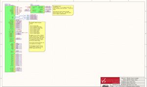
- On the Topsheet, you'll notice some notes that provide some insight into what's going on. Feel free to read those, then delete them to provide more space on the schematic. Below, we'll go through more of what's going on on the TopSheet, and how to use it.
Using the TopSheet
The TopSheet, as mentioned, is where all of your subschematics some together and connect on a high level. Below, we'll go through some of the ways this happens.
The HONEY TopSheet features two schematic symbols -- one for the HONEY_stack.SchDoc, and one for HONEY_CAN.SchDoc. As mentioned above, you should not modify the CAN portion at all -- CAN is fully implemented for you, and altering it could prevent your board from communicating with the stack. If you're curious how it works, you're free to contact ![]() @{{{display-name}}}
@{{{display-name}}}
- The Stack symbol breaks out all of the power nets and signal nets from the stack.
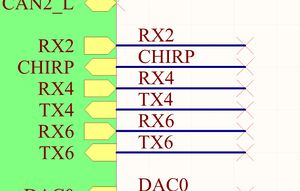
- By default, except for the power ports, everything is "disabled". This means that Altium expects none of the stuff coming out of that schematic symbol to be used. If you zoom in on the wires, you'll notice little red "X"s at the ends of them. This is something in Altium called a "Generic No ERC directive". It's a way of telling Altium -- hey, I'm not using this net, so don't worry about it. Without a No ERC directive, Altium will complain and throw compile warnings for pins that are implemented but not used.
- This is the case with all signal nets, but is no true for the power nets. By default, we've left these for you to use, but you're very likely to not use all the power nets. If you decide you aren't using a certain power net, delete the power object and replace it with a No ERC directive (this can be done by doing P->Directives->Generic No ERC) at the wire where the power port used to be.
- Otherwise, Altium assumes all the power ports are used -- if they're not, you'll get compiler errors, which should remind you to add the no ERC directive.
- As you decide to use certain signals, simply delete the Generic No ERC directive at the end of the wire, and go ahead and use it!
- You don't need to extend the wire and connect it to whatever you're doing -- in altium, you can sort of "teleport" wires by just using the same net name. That makes it cleaner.
As you start implementing stuff, you'll want to start adding more schematic sheets for your various circuits. Follow these steps:
- In your TopSheet schematic, Click P->Schematic Symbol. Then, place the symbol somewhere on your TopSheet. Drag it to whatever size square you want/need, depending on how many inputs and outputs you need to provide to that circuit from the TopSheet.
- Once it's added, modify the title (the top one of the two blue strings) to a descriptive title, and modify the filename (the bottom of the two blue strings) to "SOMETHING.SchDoc" where SOMETHING should be something descriptive about the circuit. If you want to keep following the schematic naming scheme, call it "HONEY_MYCIRCUIT.SchDoc" where MYCIRCUIT is whatever your circuit is (in a descriptive word or two).
- Once that's done, click P->Add Sheet Entry and add entries to your sheet symbol depending on what inputs/outputs your circuit in that schematic will need. Be sure to name them accordingly, and give them the appropriate direction (is this an INPUT into your circuit? an OUTPUT? or is it bidirectional?) -- this can be edited by clicking TAB while putting down the sheet entries.
- Be sure to provide power to your sheet symbol by adding sheet entries for the relevant voltage and GND.
- Once that's all done, go to the top taskbar in Altium and click "Design -> Create Sheet from Sheet Symbol" then click your newly minted sheet symbol in the TopSheet. Altium will immediately create a new schematic sheet for you, with the right name, and all of the ports in it. You're ready to add your new circuit!
There's also some minor cosmetic stuff to do to your new sheet!
- In your new schematic, use the shortcut "D->O" to open the "Document Options" screen, and then navigate to "Templates". Then, select the right template from the dropdown to have your new schematic feature the ultra beautiful SSI logo and design. You can choose between Standard, Small, and Large. Usually Small or Standard are more than sufficient. Sometimes it's buggy, and if you click the small template, it'll load the large one -- be sure to make sure the proper one loaded and change it if it didn't.
- Navigate to the "Parameters" tab. Go down to the bottom and find the "Title" parameter. Replace the asterisk with the title of this sheet. If this sheet is an atmospheric sensors schematic, you might enter "Atmospheric Sensors".
- Click OK -- you're done for now!
Finishing your design
That's all it takes to get started. Now that you're on the way to making a HONEY board, all that's left is to actually design everything. Build your circuits, add schematics, connect them, etc -- make your board! Of course, you can always ping the #altium channel in slack to get help using Altium itself.
- Once you add a schematic sheet, if you want the schematic hierarchy to update (ie to move the new sheet in the tree under the TopSheet), right click your project and click "Compile". Even if you have warnings or errors, your sheet will relocate itself properly.
- Keep adding circuits, making your design, until you're done.
- Once you're done, compile your project and get rid of any errors and whatever warnings merit attention.
Once your design compiles, there's just the icing on the cake left. You deserve to have a beautiful design to finish, so follow these steps to top it all off:
- Right click your project, and go all the way to the bottom to "Project Options".
- Go to the parameters tab.
- Update all of the fields!
- prjEngineer1 should be your name
- prjEngineer2 is anyone who helped you a lot.
- prjReviewDate might be empty for now -- make sure to get a PDR or CDR (Preliminary/Critical design review) of your board from HABEES members, then add the date here.
- prjReviewer would be whoever reviewed your design -- if many people reviewed it, list the most senior reviewer here.
- prjRevision is the same as the "generation" name you used to name your project earlier.
- prjTitle is, of course, the name of your board. For example -- HAB Avionics Gen 4.
- Click OK -- almost done!
- In the top bar, go to Tools -> Annotation -> Number Schematic Sheets
- Click all the bottoms from left to right at the bottom of the dialog
- Auto Sheet Number, then Auto Document Number, then Update Sheet Count, then OK.
- Click all the bottoms from left to right at the bottom of the dialog
- This will update all of your sheets & number them automatically.
- You're DONE with the design of your board!
Routing Your Board
Now it's time to put the design into copper. The HONEY Template already includes a HONEY-compliant PCB, so all you have to do is import your design, lay things out, connect them, and call it a day. Here's some tips and guidelines.
Making your PCB
- Once you're done with the design, double click the PCB in your folder structure -- called HONEY_TopSheet.PcbDoc to open it. (Don't rename this -- it looks for a schematic with the same name to determine what to add to the PCB -- in this case, it matches your top sheet).
- At the top of Altium, click "Design -> Import Changes From ______" where ______ will be your project name. A big window will open up.
- Click Validate Changes, and make sure everything is a green check -- if it isn't, you might have a PCB-related problem with a part or aspect of your design. Fix it or ask an Altium vet if you don't know what the error is. Fix these before proeeding.
- Click Execute Changes to import all the footprints & connections to the PCB.
- At this point, all of your stuff will be in the PCB interface.
- Now, just lay things out, and start routing! Get everything connected, and follow best practices for routing -- ask vets if you have questions.
- Note: The CAN circuit is already routed. You can change it if you really need to, but keeping it as-is ensures that everything will work as intended, since it's been routed as it should appear.
- IMPORTANT NOTE: Most PCB's made in HABEES & SSI have something called Ground Planes. These are giant pieces of copper that cover the top and bottom layers of your board, and those giant pieces of copper are connected to GND. Since they encompass your entire board, they connect everything to GND very easily -- so you don't have to route any GND pads. They are, by default, hidden, but already implemented for you in the template.
- To show them, type T->G->Restore 2 Shelved Polygons.
- As you add stuff and make changes, these ground planes will be outdated. To re-fill them and update them, type T->G->Repour All. They'll modify and fit themselves to your routing.
- Once you're done, Click Tools-> Design Rule Check.
- The DRC is a powerful but also confusing tool -- feel free to consult with vets about how to best use it, and what violations do and don't matter.
- Once you're done, and have passed DRC, make sure to add your Title box!
- The title box is a box made on the top silkscreen (In Altium, Top Overlay layer) that usually lists the name of the board, what it is, the revision & date of design, relevant engineers, a "Made with <3 in Stanford, CA" byline, a graphic picture to represent your board, and relevant sponsor logos.
- Feel free to contact vets about how to do some of this, if needed.
- The title box is a box made on the top silkscreen (In Altium, Top Overlay layer) that usually lists the name of the board, what it is, the revision & date of design, relevant engineers, a "Made with <3 in Stanford, CA" byline, a graphic picture to represent your board, and relevant sponsor logos.
Manufacturing your PCB
Once you've passed DRC, have reviewed your board, and added your title box & relevant logos, it's time to send your board to fab. Follow the following steps to make that happen.
- In your project structure, expand the "Settings" tree then expand the "Output Job Files" tree, and double click SSI.Outjob.
- This is already configured to output all of your manufacturing files, schematic sheets, and BOM as an excel sheet.
- Click "Generate Schematic PDFs" on the right hand side, then click the "Generate Content" button. Give Altium a second -- it'll make PDF's of your schematic sheets.
- Next, click the box below it, titled "Generate Manufacturing Files", then click the "Generate Content" button. Give Altium a second -- it'll produce the files for your board and a bill of materials as an excel sheet.
- You're done here -- close the outjob.
- Navigate to your project folder -- there'll be a new folder called Project Outputs for HONEY Template or possibly for SSI Template. In this folder are all of the files you just created.
- Select all of the files that are a "CAMTastic" type -- or otherwise anything ending in a .G__ extension (like GBL, GTL, etc). Then, also select the only .TXT file in the folder, which will be called HONEY_TopSheet.txt. Once this is all selected, right click and make a ZIP out of it. Call this ZIP "Gerbers_MyProject", where MyProject is the name of your project.
- That's it -- those are the files you need to make your board a reality.
- Message the HABEES lead to get final approval, and your boards will be sent out for fab.
- ONE LAST STEP!
- You need to order your parts!!
- Go to Digikey.com
- Make an account if you haven't already, then login and go to your "My Digikey" page.
- On the left hand side, go to Parts List / BOM Manager.
- Then in the right side of the table, click Create New BOM (Upload File).
- Give the BOM a descriptive name, select "XLS" as the file extension, and select your BOM from the Project Outputs directory (it's the only excel sheet).
- Then, click Upload and Map Fields.
- Digikey will ask you to map the fields
- Map the quantity field to the quantity column
- Map the Digikey part number column to the Supplier Part Number Column
- Map the Manufacturer part number column to the Manufacturer Part Number Column
- Lastly, map customer reference to the designators column -- IE the thing that says "R1, R2, C2, C4" or whatever it is -- the designators for your parts.
- That's it! Add the entire BOM to your cart after fixing problems, and order it!
- CONGRATULATIONS, YOU'VE MADE YOURSELF A HONEY BOARD!

