Hitchhiker's Guide to Making a PCB
 |
This is a guide Welcome! This article is intended to guide you through an SSI process. While its authors have made efforts to make it useful, if you have questions, please ask the authors on Slack. They will be able to both help you and improve this resource for future SSI-ers. This article was written by Sasha Maldonado ( |
|---|
Getting Started

SSI maintains Altium template PCB projects which configure a number of options to simplify the process of making a PCB. A PCB project is a type of file in Altium that organizes all of the files that go into making a real circuit board. These include all of the schematic files that define the circuits and the layout file that defines the actual geometry of the real circuit board when it's printed. The templates live in the ![]() altium-core
altium-core![]() #altium
#altium
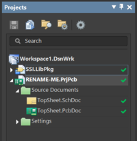
The templates are the complete folders "SSI Standard PCB Template" and "SSI Standard PCB Template - 4 Layer" - select and copy the correct folder for your board type, and paste it where you intend to work on it. On your pasted copy, rename the folder to the name of your project. Open the folder, and rename the file labeled "RENAME-ME" to the name of your project (typically with a version number - " v1" on the end). Then, open that file in Altium. You should get something that looks like the image at right in the Projects panel (if the Projects panel is not already open, go to View → Panels → Projects to open it and pin it somewhere convenient). Double click on "TopSheet.SchLib" to open it. This will produce a large, blank schematic with some default information in the lower right corner. We'll fix this information later.
Working with Schematic Sheets
Your circuit board will be electrically defined on your schematic sheet(s) - they describe what parts connect to what other parts, but not where the parts physically are on your circuit board. This abstract definition of your circuit will allow you to see where you need to draw in connections in metal when you actually begin to lay out your circuit board.
If your project is relatively simple, you should draw your entire schematic on the single TopSheet schematic document. However, if you want to reuse modular blocks (i.e. a microcontroller) from other boards, you have a meaningful amount of circuitry repeated on your board (i.e. multiple copies of the same circuit), or your board is sufficiently complicated as to not fit nicely on a single sheet, you'll want to add "subsheets." You can add sheets at any point in the design process as they become necessary, so unless you know you fall into one of the aforementioned categories, proceed by drawing your circuit on a single sheet.
Using Multiple Sheets
Altium supports hierarchical design, which has a lot of powerful features for complex designs that SSI projects don't generally need. A basic summary of hierarchical multi-sheet design is:
- All sheets have a position in the hierarchy, with one sheet at the top (hence "TopSheet.SchLib") and all other sheets one or more levels below.
- Sheets get a place in the hierarchy by being referenced with sheet symbols (see Connecting Sheets below). Any sheet that has a sheet symbol for another sheet gets a copy hierarchically beneath it. This means that your top sheet will have a sheet symbol for each second level sheet, which may each in turn have one or more lower level sheets (though this is uncommon).
- There is one unique, editable sheet file for each unique sheet in your design, but by duplicating its sheet symbol you can produce a duplicate copy of the circuit it contains in your design. This is useful for PCBs with repeated circuits - for example, ValBal avionics have two identical copies of the same motor driver circuit, one for each of the two motors in the system.
- Unless explicitly connected (see Connecting Sheets for how), wires on different sheets are not connected to each other by shared names. This means two wires labeled "SIGNAL1" on two separate sheets - even two copies of the same sheet - are not automatically connected. Importantly, this means that you need to add explicit connections for power and ground between sheets to make sure all sheets are powered.
Adding Sheets

To add a new sheet to your project, in the Projects pane, right click on your project file, go to "Add New to Project," and select "Schematic." (see right) This will create a new, blank schematic sheet in the Projects pane. The sheet will also automatically open for editing, and you'll need to save it with a descriptive file name. You'll also need to save the project file, by right clicking on it in the Projects pane and hitting "Save Project."
To reuse an existing sheet, from your file system outside of Altium, find the sheet in another project and copy it to the project folder where you want to use it. Then, in Altium, in the Projects pane, right click on your project and select "Add Existing to Project," (see right) which will bring up a new window. Find the copy you just made and select it. The sheet should then appear in the Projects pane. As with a new sheet, you'll need to save the project file, by right clicking on it in the Projects pane and hitting "Save Project."
Connecting Sheets

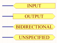
After adding a sheet (whether new or reused), you will need to connect it into your design (see above). To pass wires (i.e. power, ground, and signals of interest) between your sheet and another, your new sheet will need to have ports. Ports are placed using Place → Port. (shortcut ![]() p → r
p → r
Applying the SSI Schematic Template
This step is cosmetic and should be skipped and asked about on Slack if you can't get it to work in one attempt
To get the SSI schematic template on your sheet, you'll need to apply the template. In Altium 18 and later, there's a template drop-down in the Properties pane, in the "Page Options" section. In earlier versions of Altium, this dropdown is in the "Document Options" menu, under "Design" (shortcut ![]() d → o
d → o
Entering Project Parameters
To replace the default text on your PCB and in the schematic template, go to Project → Project Options (shortcut ![]() c → o
c → o
![]() This Altium-related article is a stub. You can help SSI by expanding it.
This Altium-related article is a stub. You can help SSI by expanding it.
