Releasing a Board for Manufacture
 |
This is a guide Welcome! This article is intended to guide you through an SSI process. While its authors have made efforts to make it useful, if you have questions, please ask the authors on Slack. They will be able to both help you and improve this resource for future SSI-ers. This article was written by Sasha Maldonado ( |
|---|
All done with your PCB? Time to get it sent out for manufacturing and to order components and a stencil!
Wait, What? I Thought I Was Done!
PCB manufacturers require special files in order to actually make circuit boards. These files describe where to place and remove copper on each layer of the board, where to drill holes, and where to expose copper and draw artwork on the outsides of the board. There are several different formats that manufacturers will accept; for SSI's leading manufacturer (Bay Area Circuits, one of our oldest and most supportive sponsors), we export Gerber files, which are machine-readable descriptions of what should be manufactured on each layer of the board. You'll also export a plain text file with coordinates for drilled holes (and what size drill bit to drill them with). These are the files required for a manufacturer like Bay Area Circuits to actually create a PCB.
Your PCB, however, will ship from the manufacturer without any components attached. If, as in most cases, you're assembling a board yourself, you'll (usually) need two additional things: components, which we generally buy from Digikey (but sometimes elsewhere, as needed - see Recommended PCB Component Suppliers if you're curious); and a stencil to help apply solder paste to your board for attaching components, which we usually buy from OSHStencils. Digikey accepts Excel spreadsheets specifying the type and number of components needed to build your board, and OSHStencils uses aforementioned Gerber files to laser cut either polyimide (Kapton) film or thin stainless steel.
To recap, you will need three things:
- A collection of Gerber files (and a text file) to send to Bay Area Circuits (or another PCB manufacturer)
- A smaller collection of Gerber files to send to OSHStencils
- An Excel spreadsheet (called a Bill of Materials, or BoM) to upload to Digikey (or manually order from other vendors)
Luckily, we have a system for producing all of the above! Enter the outjob.
SSI.OutJob
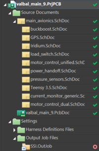
There are a number of things to configure to get Altium to correctly output Gerbers and other files. These have been fortunately taken care of and saved in a special Altium file called an outjob. You'll need to add the outjob file to your project (as if it were a schematic file), and will then be able to output files for fabrication with a couple of clicks.
Master copies of the outjobs are in the SVN at ![]() altium-core/libraries/outjobs
altium-core/libraries/outjobs![]() altium-core/libraries/templates
altium-core/libraries/templates
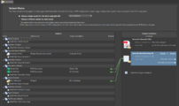
Once you have the outjob in your project and are ready to export files, open the outjob by double-clicking on it from the Projects pane. This will produce a screen like the first one below:
This outjob has the "Generate Manufacturing Files" option selected on the right side and has all three outputs - Gerbers, a drill file, and an Excel bill of materials - enabled. From here, either click the "Generate content" button under "Generate Manufacturing Files" or hit the F9 key, and Altium will produce output files (yes, it is that simple!). Outputs will be placed in your project folder inside of a new subfolder called "Fabrication Outputs." Generating all of the output files takes generally about 1 minute.
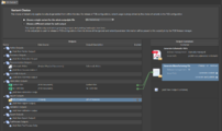
If you're in a hurry (BoM generation takes about 75% of the output file generation time) or for some other reason just want to generate Gerber and drill files and not an Excel BoM, you can disable BoM generation by clicking the little numbered circle in the Bill of Materials row. Your screen will look like the second image in the above slideshow with BoM generation disabled. To reenable BoM generation, just click the circle again.
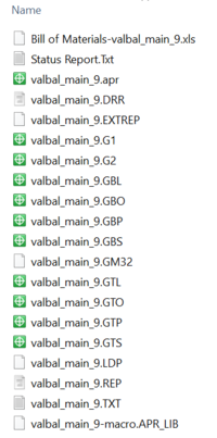
Once your fabrication outputs have been generated, find the new Fabrication Outputs folder and open it in your file browser. Add this folder to the SVN and commit it. You'll see a collection of files like the one shown at the right (with a different base name but the same file extensions). You care about the following files:
- [board].GTL - your board's top copper layer
- [board].GTS - your board's top soldermask layer, which defines what copper is exposed and solderable
- [board].GTO - your board's top silkscreen layer, which will appear as the printed artwork on the top side
- [board].GTP - your board's top solder paste layer, which will not be used to make the board but is needed for stencils
- [board].G1 (4-layer only) - your board's internal layer 1 (closer to the top side)
- [board].G2 (4-layer only) - your board's internal layer 2 (closer to the bottom side)
- [board].GBL - your board's bottom copper layer
- [board].GBS - your board's bottom soldermask layer
- [board].GBO - your board's bottom silkscreen layer
- [board].GBP - your board's bottom solder paste layer
- [board].TXT - your board's drill file
- [board].GM32 (sometimes [board].GKO) - your board's outline file
- Bill of Materials-[board].xls
You can safely ignore all of the other files (i.e. [board].apr), which are generated automatically and can't be suppressed but are not needed to manufacture a board.
For fabrication, you'll need to create a ZIP file containing all of the above files, except for the GTP/GTP files and the Excel spreadsheet (.xls). Make sure you specifically check the file extensions; several text files will be generated but there will only be one [board].txt file, which is your drill file. Give the ZIP a presentable, descriptive name that ends with "Gerbers" - it's going to be sent to a manufacturer. Also make sure you add the ZIP specifically to SVN so there's a record of exactly what was sent to the manufacturer.
Putting It All Together
We'll now describe specifically how to get each of the three things you need to assemble your board.
PCB Fabrication
This guide assumes you're ordering from Bay Area Circuits. For other manufacturers, the DfM process will be different, though you will still ultimately provide your manufacturer with your ZIP of Gerber files
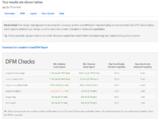
The first step in getting your board ordered is a manufacturability check, to verify you have all of the required files and the manufacturer can read them and actually make the board they describe. Bay Area Circuits (BAC) has a Design for Manufacturability (DfM) tool that automatically reads and interprets fabrication ZIPs to make sure the boards have a full set of files and can be built. Go to the InstantDfM page and follow the instructions to upload your fabrication ZIP. Once you submit, you'll have to wait usually around 10 minutes (shorter for simpler boards, longer for more complicated/four-layer boards) for processing. You'll be emailed a link when your board has finished being evaluated. The link will go to a page like the first below:
The goal is to always be within BAC's standard capabilities - this minimizes the risk of manufacturing errors and shortens production time. Small deviations (like the 0.01 mil deviation shown) come from rounding errors during the Altium export process and can be safely ignored. If truly necessary, features requiring the advanced capabilities can be produced; however this should be avoided if possible.
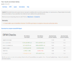
The second image in the above slideshow shows a failing DfM check. There are two major issues: first, no board outline file was included in the fabrication ZIP, meaning that BAC doesn't know what shape of board to cut. Errors like this are easy to fix by uploading a new ZIP file with all of the required files and running DfM again. Second, a hole on an inner layer does not have a copper ring, meaning that a trace on that layer won't make a good electrical connection to the hole. This is a serious issue that needs to be fixed in the design before the board is manufactured.
If your board meaningfully fails DfM for design reasons, you will need to fix the error in Altium and then repeat the outjob and DfM process. This can take some time, particularly if there are multiple issues, so make sure to budget time for DfM (especially the first time you release a board). In industrial applications, for complicated boards, it's not unheard of for a design team to spend a week verifying manufacturability; SSI designs usually pass within a few hours, and less than an hour if there are no serious problems on the first attempt.
Once you have a ZIP that passes DfM, download the InstantDfM PDF report and add it into your fabrication ZIP (to show BAC that a passing DfM was run on that board). Commit that final ZIP to the SVN, and then message ![]() #altium
#altium

