Hitchhiker's Guide to Making a PCB
 |
This is a guide Welcome! This article is intended to guide you through an SSI process. While its authors have made efforts to make it useful, if you have questions, please ask the authors on Slack. They will be able to both help you and improve this resource for future SSI-ers. This article was written by Sasha Maldonado ( |
|---|
SSI maintains Altium template PCB projects which configure a number of options to simplify the process of making a PCB. A PCB project is a type of file in Altium that organizes all of the files that go into making a real circuit board. These include all of the schematic files that define the circuits and the layout file that defines the actual geometry of the real circuit board when it's printed.
Getting Started

The templates live in the ![]() altium-core
altium-core![]() #altium
#altium
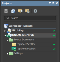
The templates are the complete folders "SSI Standard PCB Template" and "SSI Standard PCB Template - 4 Layer" - select and copy the correct folder for your board type, and paste it where you intend to work on it. On your pasted copy, rename the folder to the name of your project. Open the folder, and rename the file labeled "RENAME-ME" to the name of your project (typically with a version number - " v1" on the end). Then, open that file in Altium. You should get something that looks like the image at right in the Projects pane (if not already open, go to ![]() v → "Panels" → p
v → "Panels" → p
