Gen 2 Architecture: Difference between revisions
No edit summary |
|||
| (14 intermediate revisions by the same user not shown) | |||
| Line 1: | Line 1: | ||
{{ | {{HONEY-sidebar | ||
| header = HONEY | | header = HONEY Architecture | ||
| img link = File: | | img link = File:HONEY2.jpg | ||
| designer = Kirill Safin | | designer = Kirill Safin | ||
| techline = Balloons Core Architecture | | techline = Balloons Core Architecture | ||
| version = Generation II | | version = Generation II | ||
| name = HONEY | | name = HONEY | ||
| | | acronym = Hardware Optimized Nested Electronics sYstem | ||
}} | }} | ||
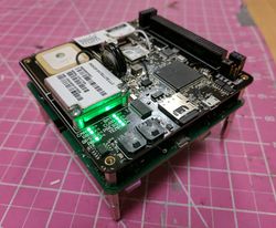
'''HONEY (Hardware Optimized Nested Electronics sYstem)''' is the second generation Core Flight Architecture, designed by HABEES. The HONEY architecture makes significant changes and improvements on the Generation I Architecture, including changes in physical dimensioning, stacking connectors, common power and data buses, and more. | '''HONEY (Hardware Optimized Nested Electronics sYstem)''' is the second generation Core Flight Architecture, designed by HABEES. The HONEY architecture makes significant changes and improvements on the Generation I Architecture, including changes in physical dimensioning, stacking connectors, common power and data buses, and more. | ||
| Line 14: | Line 15: | ||
== Physical Specifications == | == Physical Specifications == | ||
The HONEY architecture physical specifications comprise two categories: board specifications and stack specifications. | The HONEY architecture physical specifications comprise two categories: board specifications and stack specifications. | ||
=== Board Specification === | === Board Specification === | ||
| Line 192: | Line 192: | ||
|NO | |NO | ||
|- | |- | ||
|29-36, 38- | |29-36, 38-40 | ||
|IO/1 - IO/13 | |IO/1 - IO/13 | ||
|These are GPIO pins directly connected to the Core Avionics. These can be used to transfer a digital signal to the avionics, have the avionics sample an analog signal, or have the avionics PWM a signal, depending on the specific GPIO pin used. If this functionality is desired, one should reference the Core Avionics schematic to determine the pin capabilities of each of the GPIO's. These can be used both as inputs (to the Core Avionics) or outputs (from the Core Avionics). On the schematic symbol for the HABEES stackup, these are referred to as "AV____" where ____ is the corresponding pin on the Main Avionics MCU (a teensy 3.6). Reference the ____ pin on the 3.6 schematic to determine its functionality. | |These are GPIO pins directly connected to the Core Avionics. These can be used to transfer a digital signal to the avionics, have the avionics sample an analog signal, or have the avionics PWM a signal, depending on the specific GPIO pin used. If this functionality is desired, one should reference the Core Avionics schematic to determine the pin capabilities of each of the GPIO's. These can be used both as inputs (to the Core Avionics) or outputs (from the Core Avionics). On the schematic symbol for the HABEES stackup, these are referred to as "AV____" where ____ is the corresponding pin on the Main Avionics MCU (a teensy 3.6). Reference the ____ pin on the 3.6 schematic to determine its functionality. | ||
|NO | |||
|- | |||
|41 | |||
|BLUEJ_PRESENT | |||
|This pin is pulled high by the BlueJay RockBlock breakout board -- to signal to the main avionics that it is in use, as opposed to the on-board 9603 modem. | |||
|NO | |||
|- | |||
|81-86 | |||
|RB Breakout | |||
|These pins are connected to the avionics RockBlock signal lines -- including TX, RX, SLP, NETAV, ENABLE, and RING INDICATOR. They are meant to allow the avionics to use an external RockBlock breakout board instead of its on-board 9603 modem, or, in the future, to allow the RockBlock to be broken out from the avionics if desired. They should not be touched by anything except the avionics. In this breakout, TX connects to an MCU TX, and RX connects to an MCU RX (as opposed to the standard swapped interface). | |||
|NO | |NO | ||
|- | |- | ||
| Line 276: | Line 286: | ||
|IO/12 | |IO/12 | ||
|- | |- | ||
| | |BLUEJ_PRESENT | ||
|RESERVED | |RESERVED | ||
|RESERVED | |RESERVED | ||
| Line 326: | Line 336: | ||
|RESERVED | |RESERVED | ||
|- | |- | ||
| | |RB_TX --> | ||
| | |RB_RX <-- | ||
| | |RB_NETAV | ||
| | |RB_SLP | ||
|- | |- | ||
| | |RB_RI | ||
| | |RB_EN | ||
|RESERVED | |RESERVED | ||
|RESERVED | |RESERVED | ||
| Line 462: | Line 472: | ||
#Make sure +3.3_CAN is used only to power the transceiver, and nothing else. | #Make sure +3.3_CAN is used only to power the transceiver, and nothing else. | ||
#Make sure CAN_SPD is hard-wired to the transceiver speed pin. | #Make sure CAN_SPD is hard-wired to the transceiver speed pin. | ||
[[Category: High Altitude Balloons]][[Category: HABEES]][[Category: HONEY]] | |||
Latest revision as of 22:41, 31 August 2017
| HONEY Architecture | |
|---|---|
| Part of the HONEY Architecture series & the HABEES series | |
| |
| Chief Designer | Kirill Safin |
| Technology Line | Balloons Core Architecture |
| Version | Generation II |
| Name | HONEY |
| Acronym | Hardware Optimized Nested Electronics sYstem |
| General | |
| HONEY Standards • Venom Breakout • Fang Breakout • Board Naming | |
| Core Software | |
| STINGR | |
| Core Avionics | |
| The Count | |
| Core Power | |
| Biscuit | |
| Core Peripherals | |
| Cobra • Viper • ProtoBee | |
| Core Radio | |
| Macaw | |
| Test & Prototype | |
| QueenBee | |
| Guides | |
| Making a HONEY Board • Using STINGR • Using QueenBee • Making a Prototype | |
| V • E | |
HONEY (Hardware Optimized Nested Electronics sYstem) is the second generation Core Flight Architecture, designed by HABEES. The HONEY architecture makes significant changes and improvements on the Generation I Architecture, including changes in physical dimensioning, stacking connectors, common power and data buses, and more.
The HONEY specification is outlined below in exhaustive detail, and the bottom of the page lists implementations required by any board utilizing the HONEY architecture.
Physical Specifications
The HONEY architecture physical specifications comprise two categories: board specifications and stack specifications.
Board Specification
All boards implementing the HONEY spec must meet strict physical requirements. There is a standardized set of measurements, mounting holes, connector placements, and board dimensions that must be met for proper integration with the flight stack.
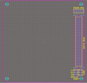
The dimensions of a HONEY-compliant board are exactly 10x10 cm. Boards are 0.062" in thickness (this is important for the physical fastening of the flight stack to the payload container, which is sensitive to the thicknesses of boards in the flight stack. Boards also have four through-holes at each corner, designated for standoffs. The holes are designed for M3 standoffs, which are indented 250 mil from both edges of the respective corner. The board also necessarily consists of a PC/104+ connector for the flight stack data bus, a 10-pin (5x2) connector for the flight stack power bus, a 6-pin (3x2) connector for the flight stack CAN bus, and an 8 pin (4x2) connector (NON stack through) for holding jumpers for implementing CAN terminating impedances. These connectors are not physically located on the board in a whole-number fashion, but must be implemented with exact precision to allow for proper stack-through ability. The PC/104+ connector also comes with a paired shroud that clips onto the board via four through-holes, which, while not strictly required for operation, is highly encouraged and is part of the stack-up Altium part. Boards are expected to not exceed their boundaries by more than 0.25". The flight stack has 0.5" of space around it, between its outer dimensions and the walls of the payload container.
The connectors and hardware used in each case can be found on the HONEY Standardized Connectors Page
- Data Bus: Harwin M22-6003005
- Data Bus Shroud: Harwin M22-6043098
- Power Bus: Samtec ESQ-105-38-G-D-LL
- CAN Bus: Samtec ESQ-103-38-G-D-LL
- CAN Jump Holder: Samtec TSW-104-07-G-D
- CAN Terminating Jumper: Samtec SNT-100-BK-T
- Stack Standoffs: Harwin R6104-02
The physical footprint of a HONEY base-board can be found in the Altium library as "HABEES STACKUP" -- this features both a compliant and properly dimensioned PCB PCB, as well as a schematic symbol for accessing the power, data, and CAN buses.
Stack Specification
The HONEY architecture is defined by a flight stack, comprised of stacked HONEY-compliant boards, with common data, power, and CAN buses, physically integrated through a series of four corner standoffs. Flight boards in the flight stack are inter-connected by the standoffs mentioned above (Harwin R6104-02 standoffs). Boards are expected to be 0.062" thickness.
The flight-stack is compromised of two primary divisions: Flight Critical Components (FCC) and Flight Tertiary Components (FTC). At time of writing, there are only two FCC's -- the Core Avionics and the Core BMS. All other boards, non-essential to flight operation, are considered FTC. Components are categorized and assessed as FCC or FTC upon design and implementation on a rolling basis. A flight-ready flight-stack must consist of at least one of each of the Flight Critical Components, and can include zero or any number of Tertiary Flight Components.
As of writing, The FCC (Avionics & BMS) are specified by the HONEY spec as being the strictly top-most and strictly bottom-most boards in the flight stack, with all FTC in-between. This is the case for two reasons: Core Avionics required a clear view of the sky for proper Iridium & GPS reception, and therefore must be on the top of the stack. The BMS holds four 18650 Li-Ion cells on its bottom, and the standard inter-board spacing is insufficient to fit the battery pack. it is therefore allocated to the bottom of the stack, which is fastened to the payload container by longer standoffs to accommodate the battery pack size.
The flight stack is therefore comprised of a minimum of two boards, and can theoretically be any defined height. Currently, a flight stack of five boards is categorized as a "1U flight-stack" for payload-integration purposes. An additional sixth board results in a 2U flight stack, an eleventh board results in a 3U flight stack, and so on.
As defined by the current spec, the physical stack dimensioning is as so:
- XY-Board Dimensions: 10x10 cm
- Z-Board Thickness: 0.062"
- Permissible Extension outside of Board Dimensions: 0.25"
- Maximum spacing outside of Board Dimensions: 0.5"
- Inter-Board spacing: 15.24mm, as defined by the Harwin R6104-02 standoff.
- BMS-Payload Base spacing: 25mm, as defined by McMaster 94868A013, 10/12mm standoffs (McMaster 92005A120, 92005A122)
- Avionics-Roof spacing: Variable, depending on stack height.
Avionics-Roof spacing, by stack height:
- 2-Boards (Base Stack): 51mm spacing, 60mm fixture bolt. (McMaster 94669A127, 92005A140)
- 3-Boards (Base + 1 FTC): 35mm spacing, 45mm fixture bolt. (McMaster 94669A121, 92005A136)
- 4-Boards (Base + 2 FTC): 16mm spacing, 30/25mm fixture bolt. (McMaster 94669A111, 92005A132, 92005A130)
- 5-Boards (Base + 3 FTC): 25mm spacing, same as BMS. (McMaster 94868A013, 92005A120, 92005A122)
Electrical Specifications
The HONEY architecture defines pinouts for the various bus connectors, as well as pins required for implementation and auxiliary pins one can use on a given stack-board.
There are three defined buses, with specific purposes, limitations, and requirements as defined by the HONEY electrical specification.
Power Bus
The power bus pin-out is as follows:
| 3.3V | 5V | VBATT | VADJ | GND |
| 3.3V | 5V | VBATT | 1.8V | GND |
The purpose of the power bus to supply power to the entirety of the flight-stack. It does this using high-current rated pins, ultimately deriving their power from the BMS. At the time of writing, the active BMS is Biscuit, and the following will be written with the Biscuit specifications.
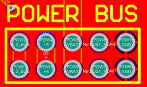
The power bus provides a +5V supply, with a flight-stack current limit of 4A -- this voltage should be used for devices that specifically require 5 volts (such as Iridium), or in many cases for more localized and low-noise voltage regulation on individual boards (i.e. LDO'ing the 5V to 3.3V for a local Teensy).
The power bus provides a +3.3V supply, with a flight-stack current limit of 1A -- this voltage should be used for powering most low-power logic-level devices, and in many cases embedded Teensies as well. At time of writing, Biscuit is still being brought to operating state, and all FTC's are advised to either regulate 3.3V locally, or have a switch for selecting between BUS +3.3 and local +3.3 -- this is done on Macaw, which can be looked at as an example. Ideally, all +3.3 devices run on the BMS supplied +3.3V.
The power bus also provides raw cell voltage +VBATT -- this voltage is nominally 3.7V, 4.25V at full capacity, and changes from ~ 4.25V down to ~ 3.2V at pack end-of-life. It's purpose is strictly for high current applications where high power with few voltage requirements is the defining characteristic. The pack can source ~ 12 amps from the VBATT line at peak (should not be tapped at this current for too long). Examples of its current application are for nickel chromium cutdown (1A), and in-board heaters for the BMS and Avionics (~ 500 mA), as well as powering the Dorji Radio Transceivers on Macaw (1W @ 4.2V).
The power bus also provides two utility regulators -- 1.8V for specific 1.8V applications for some specialty IC's (250 mA limit), and an adjustable buck that regulates to a voltage between 0V and 5V, as dictated by the Avionics. The Avionics is solely responsible for regulating the adjustable voltage, using the VA_PWM pin on the data bus -- if your board necessitates an adjustable voltage, it must request the adjustment via the avionics, which will either accept or deny the request, and act accordingly.
Lastly, the power bus provides two nodes for common ground, which must be implemented to common-ground a board to the BMS/flight-stack.
Data Bus
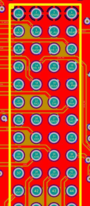
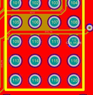
The data bus serves as a means by which to transfer specific reserved signals throughout the flight stack, access reserved Core Avionics UART lines, as well as Core Avionics SPI/I2C, as well as implement system flags, and some other utility features. While primary communication between boards happens via the CAN bus, certain pins on the data bus are required to be implemented by all boards in the flight stack, and other pins may yield utility, depending on the specific application of a board. All "RESERVED" pins currently serve no purpose, and may be reserved by your board for transitioning signals up and down the flight stack. A number of pins will, in the future, become tertiary power pins for advanced BMS applications. These will likely occupy the bottom of the data bus. Pins on the data bus are to be occupied on a top-down basis, filling from top-down and left-right, with the exception of RESERVED pins that are amidst dedicated pins, which are strictly reserved for possible future flight-critical services.
A description of all the pins and whether they are required to be implemented is found in the following table, and the entire pinout can be found following this table.
| Pin | Net | Purpose | REQ? |
| 1-4 | GND | GND | YES |
| 5 | VBCKP | The VBCKP pin is connected to a +3V coin cell located on the BMS. This pin serves as a backup, low-current 3V supply primarily for memory applications, such as RTC's & GPS memory. It continues to power crystals and internal memory to keep the state of RTC's, etc, even through power-cycles. | NO |
| 6 | R_MCU | The R_MCU pin, if pulled high, resets the Core Avionics board remotely. This pin should be implemented under almost NO CIRUMSTANCES. The Avionics largely in charge of the flight stack, and very few boards should ever have the authority to reset it. It exists for possible, if seldom, application. | NO |
| 7 | R_ALL | The R_ALL pin, if pulled high, will reset all boards in the flight stack. This pin is controlled exclusively by the Core Avionics, and should be tied to the reset pin of any MCU found on a board. The Avionics has the authority to reset all flight stack boards in the case of excessive power consumption, poor responsiveness, or erratic behavior. | YES |
| 8 | S_READY | The S_READY pin, once pulled high, alerts all flight stack boards that the Core Avionics has passed initial booting, and is ready to accept requests and provide flight services. All boards should wait until S_READY is high to begin their initialization and operating procedures. | YES |
| 9 | LOW_PWR | The LOW_PWR pin, once pulled high, alerts all flight stack boards that they should enter low power mode, whereby they should conduct all possible actions to minimize power consumption. This flag is pulled high in the case that the payload is losing power, and must retain all power for flight critical operations. | YES |
| 10 | FMODE | The FMODE pin, once pulled high, alerts all flight stack boards that the payload has been released, and is ascending, and in flight mode. This is a utility flag that can be implemented if your board desires to know whether flight has begun, or whether the payload has not yet been released, or has landed. | YES |
| 11-14 | SYS_F(3-6) | Reserved System Flags for future purposes. | YES |
| 15, 16 | SDA/SCL | These pins provide access to the Core Avionics I2C bus. This should be used in very extenuating circumstances, when Core Avionics control over an I2C device on a board is desired. | NO |
| 17-19 | SPI | These pins provide access to the Core Avionics SPI bus. This should be used in very extenuating circumstances, when Core Avionics control over an SPI device on your board is desired. | NO |
| 20 | VA_PWM | This pin is a pulse-width modulated pin, controlled exclusively by the avionics, that adjusts the VADJ voltage, found on the power bus. While a board can technically implement this pin, VADJ control is exclusively in the hands of the avionics, and nobody should attempt to modulate this pin. | NO |
| 21 | CHIRP | This pin is a UART TX pin from the Core Avionics, on which the Core Avionics will transmit a regular status message to the entire flight stack. This message will consist of information of various payload vitals, such as internal/external temperature, altitude, ascent rate, lat, long, etc. While not required, it is highly recommended to implement this pin for the purpose of being able to receive the broadcast message and have high-level flight awareness for a board. The board can specifically request data over CAN, if it chooses. | YES |
| 22 | RX2 | This pin is the RX partner of the CHIRP pin, which has no likely purpose, and should not be implemented. | NO |
| 23/24 | UART4 | This provides access to the Core Avionics Hardware UART #4 -- this should not be utilized unless expressly agreed upon, as it alters the architecture definition and devotes this UART specifically for one board. | NO |
| 25/26 | UART6 | This provides access to the Core Avionics Hardware UART #6 -- this should not be utilized unless expressly agreed upon, as it alters the architecture definition and devotes this UART specifically for one board. | NO |
| 27/28 | DAC0/1 | These pins provide access to the two Core Avionics DAC outputs. These should be used strictly as input pins -- if a board requires an analog signal to be produced, it should notify the Core Avionics of the desired signal, desired DAC channel for output, and use the output. | NO |
| 29-36, 38-40 | IO/1 - IO/13 | These are GPIO pins directly connected to the Core Avionics. These can be used to transfer a digital signal to the avionics, have the avionics sample an analog signal, or have the avionics PWM a signal, depending on the specific GPIO pin used. If this functionality is desired, one should reference the Core Avionics schematic to determine the pin capabilities of each of the GPIO's. These can be used both as inputs (to the Core Avionics) or outputs (from the Core Avionics). On the schematic symbol for the HABEES stackup, these are referred to as "AV____" where ____ is the corresponding pin on the Main Avionics MCU (a teensy 3.6). Reference the ____ pin on the 3.6 schematic to determine its functionality. | NO |
| 41 | BLUEJ_PRESENT | This pin is pulled high by the BlueJay RockBlock breakout board -- to signal to the main avionics that it is in use, as opposed to the on-board 9603 modem. | NO |
| 81-86 | RB Breakout | These pins are connected to the avionics RockBlock signal lines -- including TX, RX, SLP, NETAV, ENABLE, and RING INDICATOR. They are meant to allow the avionics to use an external RockBlock breakout board instead of its on-board 9603 modem, or, in the future, to allow the RockBlock to be broken out from the avionics if desired. They should not be touched by anything except the avionics. In this breakout, TX connects to an MCU TX, and RX connects to an MCU RX (as opposed to the standard swapped interface). | NO |
| 105-108 | 12V | These pins, although on the databus, provide 12V power for 12V applications -- when used, all four nets should be connected together and used in parallel. | NO |
| 113/114 | (+5V and -5V) (SIG) | These pins are meant to be used for signal applications requiring a dual polarity +5V to -5V rail-to-rail supply. They only put out 15 mA, and should not be used for any power applications whatsoever. | NO |
| 115/114 | (+12V and -12V) (SIG) | These pins are meant to be used for signal applications requiring a dual polarity +12V to -12V rail-to-rail supply. They only put out 15 mA, and should not be used for any power applications whatsoever. | NO |
| 37, 42-111, 117-120 | NC | Reserved -- these can be used for any purpose at the time being, as long as it is agreed in advance. | NO |
| 112 | CAN_SPD | This pin, controlled by the Core Avionics, determines the current speed of the flight stack CAN bus. This pin should be directly tied to the speed-select pin of the CAN Transceiver on a given board. No board should control this pin in any way, except to feed it in this fashion. The Core Avionics will adjust the speed of the CAN Bus as necessary, thereby adjusting all board Transceivers simultaneously. | YES |
| GND | GND | GND | GND |
| VBCKP | R_MCU | R_ALL | S_READY |
| LOW_PWR | FMODE | SYS_F3 | SYS_F4 |
| SYS_F5 | SYS_F6 | SDA | SCL |
| MOSI | MISO | SCLK | VA_PWM |
| CHIRP | RX2 | TX4 | RX4 |
| TX6 | RX6 | DAC0 | DAC1 |
| IO/1 | IO/2 | IO/3 | IO/4 |
| IO/5 | IO/6 | IO/7 | IO/8 |
| RESERVED | IO/10 | IO/11 | IO/12 |
| BLUEJ_PRESENT | RESERVED | RESERVED | RESERVED |
| RESERVED | RESERVED | RESERVED | RESERVED |
| RESERVED | RESERVED | RESERVED | RESERVED |
| RESERVED | RESERVED | RESERVED | RESERVED |
| RESERVED | RESERVED | RESERVED | RESERVED |
| RESERVED | RESERVED | RESERVED | RESERVED |
| RESERVED | RESERVED | RESERVED | RESERVED |
| RESERVED | RESERVED | RESERVED | RESERVED |
| RESERVED | RESERVED | RESERVED | RESERVED |
| RESERVED | RESERVED | RESERVED | RESERVED |
| RB_TX --> | RB_RX <-- | RB_NETAV | RB_SLP |
| RB_RI | RB_EN | RESERVED | RESERVED |
| RESERVED | RESERVED | RESERVED | RESERVED |
| RESERVED | RESERVED | RESERVED | RESERVED |
| RESERVED | RESERVED | RESERVED | RESERVED |
| RESERVED | RESERVED | RESERVED | RESERVED |
| 12V | 12V | 12V | 12V |
| RESERVED | RESERVED | RESERVED | CAN_SPD |
| Pos 5V (SIG) | Neg 5V (SIG) | Pos 12V (SIG) | Neg 12V (SIG) |
| RESERVED | RESERVED | RESERVED | RESERVED |
CAN BUS
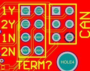
The CAN bus is the primary means of communication within the flight stack. The CAN bus is the means by which any board can request data from the avionics, receive data from the avionics, as well as receive commands and requests from the avionics for a specific action.
Every board, except in very extenuating circumstances, is required to implement the CAN bus.
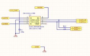
The required, standardized HONEY transceiver is the TI_SN65HVD230.
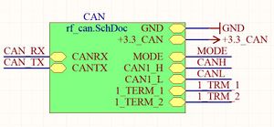
There are two CAN buses -- CAN1 and CAN2. CAN1 is the primary CAN bus used for the flight stack, while CAN2 is a secondary bus that exists only for possible future use. All boards should implement CAN1. The schematic for the CAN system for each board is well defined, and should be implemented exactly as shown. The CAN connector, in addition to the above described four nodes, includes a +3.3_CAN pin and a GND pin. GND should be common grounded, while +3.3_CAN should be used to power the CAN transceiver -- it should power no other device on a board, and the CAN transceiver should exclusively use this pin as its power source.
Shown here is the CAN schematic that should be implemented on any board.
| CAN1_H | CAN1_L |
| CAN2_H | CAN2_L |
| 3.3V_CAN | GND |
CAN Terminating Jumpers
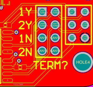
The CAN Terminating Impedance Connector, a 2x4 male terminal strip, is used for the purpose of applying the necessary 120-ohm terminating impedance on each end of the CAN bus. Since the current HONEY architecture dictates that the Core Avionics and Core BMS occupy the top and bottom positions in the stack, they are currently the only boards to utilize this connector. However, as the architecture may evolve, and positions of boards change, it is necessary to implement this connector so that your board may effectively institute the necessary terminating impedance.
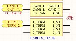
A CAN bus requires a 120 ohm resistor between CAN HIGH and CAN LOW for the first and last devices on the bus to prevent reflections. This is achieved by jumping two pins, with a resistor in between. In this case, for CAN1, this is achieved by the top two pins in this connector. 1_TERM_1 and 1_TERM_2 are open-circuit, but, when jumped, become closed. 1_TERM_2 is connected to CAN1_L. 1_TERM_1 is connected to one end of a 120 ohm resistor -- the other end of the resistor is connected to CAN1_H. Thereby, by placing a jumper on the two pins and closing the circuit, a 120 ohm impedance is effectively engaged, properly terminating the bus. The same is true for pins 3/4, which are for CAN2 (not used by most boards). Pins 4-8 exist solely as a position to place jumpers when they are not used by a board -- IE when the board is not implementing the terminating impedance.
The schematic for the implementation of this connector, including both the relevant portion of the stack connector, and its connection to the CAN transceiver, is shown here.
| 1_TERM_1 | 1_TERM_2 |
| 2_TERM_1 | 2_TERM_2 |
| NC | NC |
| NC | NC |
Software Specification
HONEY implements a flight stack-wide software suite called STINGR (Stack Transmission & Inter-Nodal Gesture Repository, which provides a variety of function calls, interrupt handlers, and error-handling for communication within the stack, primarily utilizing the CAN Bus.
The full STINGR specification can be found on the STINGR page.
Implementation
Below is a short guide/list of steps to guide the design and implementation of a board for the HONEY architecture. One should follow it carefully, as it is specifically written to prevent one from making mistakes by forgetting to implement a required functionality, or using a restricted functionality.
Required Implementation
- Use the latest HABEES_STACK_TEMPLATE part from the Altium library. This is to be kept updated by HABEES members to reflect changes in pinout, physical layout, etc, and is required to make your board meet the physical and electrical bare requirements.
- Common Ground all GND nets on the stack connectors to your GND -- this includes two on the Power Bus, four on the Data Bus, and one on the CAN bus.
- For the nets of the power bus that your board is utilizing, make sure to electrically short the nets together, and join them by a 40/50-mil trace. The reason there are two pins is to provide a higher current-limit, so you should tie them together to ensure proper rating.
- Make sure to NOT IMPLEMENT any of the following restricted pins, unless specifically agreed upon in advance (don't touch them at all, even as an input) -- 6 (R_MCU), 22 (RX2) 112 (CAN_MODE -- this shouldn't go anywhere except your Transceiver)
- Make SURE TO IMPLEMENT the following pins as INPUTS to your MCU -- 7 (R_ALL), 8 (S_READY), 9 (LOW_PWR), 10 (FMODE), 11-14 (System Flags 3-6, reserved), 21 (CHIRP -- should go to a Serial RX pin on your MCU).
- Make sure to properly implement the CAN Bus -- duplicate the existing schematic for the primary circuit, and verify that you have properly implemented the terminating impedance sub-circuit.
- Be sure to connect pin 112 (CAN_SPD) from the data bus to the speed pin on your CAN Transceiver. Without this, it will not function.
- Be sure to use +3.3_CAN pin from the CAN Bus EXCLUSIVELY to power your Transceiver, and make sure it powers nothing else.
- Make sure pin 7 (R_ALL) is directly wired to your MCU reset pin, to allow Core Avionics remote reset.
- If using RTC, make sure to implement pin 5 (+VBCKP).
- Make sure no component of the board extends more than 0.25" over the board edge.
Self-Help FAQ
- If implementing the data bus SPI or I2C lines, this should be agreed upon by current HABEES members as an appropriate use of the Core Avionics I2C/SPI buses before action is taken.
- If using either of the dedicated Core Avionics Hardware UARTs (pins 23/24 and 25/26), this should be agreed as constituting a reasonable use -- being that it is critical enough to warrant their use, or otherwise cannot be achieved.
- If using either DAC (pins 27 and 28) verify it can only be used as an input, and will not be used in any way as an output (IE do not output to those pins).
- If using any of the Core Avionics GPIO's on the data bus (pins 29-36, 38-41), be sure that it isn't currently being used by another board (unless you specifically want it to be, such as using the pin as a feed-through signal line), whether the pin is able to perform the desired action (PWM, ADC, DIO), and agree amongst HABEES members that it is a reasonable and just usage of the pin, which would henceforth be reserved for your purpose.
- If using any of the current RESERVED pins (37, 42-111, 113-120), agree amongst HABEES members that it is a just and fair usage of the pin, which would henceforth be reserved for your purpose.
- Make sure, unless for some reason you're using it, CAN2 is not connected to anything.
- Make sure +3.3_CAN is used only to power the transceiver, and nothing else.
- Make sure CAN_SPD is hard-wired to the transceiver speed pin.
