Making Parts for PCB Libraries: Difference between revisions
Smaldonado (talk | contribs) Added some detail to the schematic section, a bunch of material to the footprint section |
Smaldonado (talk | contribs) Populated "Finishing a Component" |
||
| Line 6: | Line 6: | ||
Altium has several different noteworthy types of libraries. | Altium has several different noteworthy types of libraries. | ||
* '''Schematic libraries''' (.SchLib files) store schematic symbols and the components they correspond with. Schematic libraries contain schematic editor symbols, links to footprints (from PCB libraries; see below), mapping between the pins in the schematic symbol and pads on the footprint, and links to the part supplier (most often, | * '''Schematic libraries''' (.SchLib files) store schematic symbols and the components they correspond with. Schematic libraries contain schematic editor symbols, links to footprints (from PCB libraries; see below), mapping between the pins in the schematic symbol and pads on the footprint, and links to the part supplier (most often, Digi-Key) | ||
* '''PCB libraries''' (.PcbLib files) contain the actual PCB layouts for library components. PCB libraries include landing patterns (the actual pad shapes that will appear on the PCB) and 3D models of the associated packages. | * '''PCB libraries''' (.PcbLib files) contain the actual PCB layouts for library components. PCB libraries include landing patterns (the actual pad shapes that will appear on the PCB) and 3D models of the associated packages. | ||
* '''Integrated libraries''' (.LibPkg files) are Altium projects that combine schematic and PCB libraries. | * '''Integrated libraries''' (.LibPkg files) are Altium projects that combine schematic and PCB libraries. | ||
| Line 26: | Line 26: | ||
Next, you'll draw out the graphics for your symbol. Begin by setting the snap grid of the editor (the grid of points it will allow for drawing) to 10 point spacing, by opening the snap grid settings {{altium-shortcut|v|g|s}} and entering 10 for the snap grid size. This is not strictly required, and smaller grids can be used to create finer detail in symbols (5 and 2.5 are recommended), but all connection points for the symbol (added later) must be placed on a 10 point grid and thus symbols should be drawn to accommodate that. | Next, you'll draw out the graphics for your symbol. Begin by setting the snap grid of the editor (the grid of points it will allow for drawing) to 10 point spacing, by opening the snap grid settings {{altium-shortcut|v|g|s}} and entering 10 for the snap grid size. This is not strictly required, and smaller grids can be used to create finer detail in symbols (5 and 2.5 are recommended), but all connection points for the symbol (added later) must be placed on a 10 point grid and thus symbols should be drawn to accommodate that. | ||
For logic gates, transistors, and other components that traditionally have distinct schematic symbols, it is helpful to draw those symbols - you can often copy the graphics from an existing, similar part by simply opening the existing part from the symbols list in the SCH Library pane, selecting all of the symbol in the editing window and copying, then reopening and pasting into your own symbol. You should then delete all of the pins and replace them as described below. If no suitable symbol exists, draw a symbol by placing lines {{altium-shortcut|p|l}}, referring to existing symbols for guidelines on size and color. Altium's documentation of the line tool is available [http://techdocs.altium.com/display/ADRR/Sch_Obj-Line((Line))_AD here]. | For logic gates, transistors, and other components that traditionally have distinct schematic symbols, it is helpful to draw those symbols - you can often copy the graphics from an existing, similar part by simply opening the existing part from the symbols list in the SCH Library pane, selecting all of the symbol in the editing window and copying, then reopening and pasting into your own symbol. You should then delete all of the pins and replace them as described [[#Pins|below]]. If no suitable symbol exists, draw a symbol by placing lines {{altium-shortcut|p|l}}, referring to existing symbols for guidelines on size and color. Altium's documentation of the line tool is available [http://techdocs.altium.com/display/ADRR/Sch_Obj-Line((Line))_AD here]. | ||
Integrated circuits are typically represented in schematics simply with rectangles; you can place a rectangle {{altium-shortcut|p|r}} by specifying two opposite corners. Rectangles are easy to resize; it is recommended that you start with a large rectangle and downsize after placing pins. | Integrated circuits are typically represented in schematics simply with rectangles; you can place a rectangle {{altium-shortcut|p|r}} by specifying two opposite corners. Rectangles are easy to resize; it is recommended that you start with a large rectangle and downsize after placing pins. | ||
| Line 51: | Line 51: | ||
==Finishing a Component== | ==Finishing a Component== | ||
===Pairing Schematic Symbols and Footprints=== | |||
[[File:BrowseLibraries.png|300px|thumb|After clicking "Browse," this dialogue will appear. Note the dropdown containing all installed .PcbLibs]] | |||
After finishing a schematic symbol and footprint, switch to the schematic symbol in the schematic library editor. In the "Editor" pane at the bottom of the screen, click "Add Footprint," then "Browse." From there, find the relevant PCB footprint library in the dropdown, and then the relevant footprint within the library. Double click the footprint to return to the "Add Footprint" dialogue, where the selected footprint's details will now be shown. | |||
Click "Pin Map," and confirm that the pins on the schematic symbol match up appropriately with the pads on the footprint (if pins were given designators that correspond with their pad numbers, this should have happened automatically). If they don't match, edit the fields until they do. Multiple schematic pins can map to the same footprint pad, but not the other way around - for two pads to connect to the same pin, they must be given the same number in the PCB library editor. | |||
Next, click OK. Your schematic symbol is now paired with a footprint! The footprint should now show up in the list of footprints at the bottom of the Editor pane. | |||
===Adding Supplier Links=== | |||
[[File:AddSupplierLink.png|300px|thumb|Showing how to add a supplier link to a part. This supplier link, for a real Digi-Key part (a [http://www.digikey.com/product-detail/en/digi-key-electronics/CW1011/CW1011-CD/1642996 Tchaikovsky CD]) would be a very bad choice to add to an automotive capacitor symbol, as the symbol does not represent the product in question.]] | |||
The final step is to add a link to a supplier part, to allow for automated BOM ordering. Open the "Supplier Search" pane {{altium-shortcut|v|w|s|u}}, and type in either the manufacturer's part number or (better, though less universally applicable) the Digi-Key part number. A number of vendor options should appear if the part is purchasable. Most SSI electronic components are purchased in small quantities from Digi-Key; therefore, look through the list and try to find a "cut tape" (purchasable in single units) version of the part, ideally sold by Digi-Key. Then, right click (see right) and select "Add Supplier Link and Parameters to <SYMBOL_NAME>." When this completes, an entry should appear in the "Supplier" section of the SCH Library pane {{altium-shortcut|v|w|c|b}}. | |||
You're done creating this component! Save the schematic library, and proceed to the final steps below. | |||
==Recompiling and SVN Management== | ==Recompiling and SVN Management== | ||
Revision as of 20:52, 14 June 2016
This article describes how to create a new part in SSI's Altium PCB component libraries. SSI maintains a collection of Altium component libraries, many of them derived from libraries generously donated to SSI by the Stanford Solar Car Project. This is designed to serve as both a reference, and a practical guide for how to turn a component with a datasheet into a schematic symbol with a corresponding PCB footprint.
Introduction
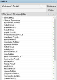
Prior to creating a part, you should have installed and configured Altium and TortoiseSVN. In Altium, open the SSI Library project - SSI.libpkg, in SSI_SVN/libraries/intlib - with File → Open Project ![]() f → j
f → j![]() v → w → s → p
v → w → s → p
Altium has several different noteworthy types of libraries.
- Schematic libraries (.SchLib files) store schematic symbols and the components they correspond with. Schematic libraries contain schematic editor symbols, links to footprints (from PCB libraries; see below), mapping between the pins in the schematic symbol and pads on the footprint, and links to the part supplier (most often, Digi-Key)
- PCB libraries (.PcbLib files) contain the actual PCB layouts for library components. PCB libraries include landing patterns (the actual pad shapes that will appear on the PCB) and 3D models of the associated packages.
- Integrated libraries (.LibPkg files) are Altium projects that combine schematic and PCB libraries.
- Compiled libraries (.IntLib files) are installable files that allow you to use library parts in schematics and PCBs. Every time a part is added to a library, the Integrated library will need to be recompiled before the part can be added to a PCB project.
Locking in SVN

Prior to adding a part to a library, it's important to "lock" the library in SVN so that other people using the library don't create a conflicted copy. Locking does keep other people from making library edits at the same time, so do not lock a library unless you will be immediately editing it, and, even if a symbol or component is not completely done, commit any libraries you've locked before stepping away for an extended period of time (see Recompiling and SVN Management). To lock any library, right click on it in the Projects pane, click "Version Control," and then "Lock" ![]() right click → e → l
right click → e → l![]() #altium
#altium
Creating a New Schematic Symbol

Drawing a Symbol
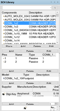
To create a new schematic symbol, first find the relevant schematic library. Schematic libraries are sorted by function - i.e. power management integrated circuits (PMIC), diodes, etc. Next, lock the library you'll be working with, and double click the library to open it. If not already visible, open the "SCH Library" pane ![]() v → w → c → b
v → w → c → b
Next, you'll draw out the graphics for your symbol. Begin by setting the snap grid of the editor (the grid of points it will allow for drawing) to 10 point spacing, by opening the snap grid settings ![]() v → g → s
v → g → s
For logic gates, transistors, and other components that traditionally have distinct schematic symbols, it is helpful to draw those symbols - you can often copy the graphics from an existing, similar part by simply opening the existing part from the symbols list in the SCH Library pane, selecting all of the symbol in the editing window and copying, then reopening and pasting into your own symbol. You should then delete all of the pins and replace them as described below. If no suitable symbol exists, draw a symbol by placing lines ![]() p → l
p → l
Integrated circuits are typically represented in schematics simply with rectangles; you can place a rectangle ![]() p → r
p → r
Pins
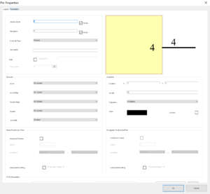
Pins are how your symbol will be connected to wires when used in schematics. Enter the pin placement tool ![]() p → p
p → p![]() tab
tab![]() tab
tab
Next, resize rectangles and lines and move pins around until you're satisfied with the look of the symbol. You're done drawing the symbol! Make sure to save the .SchLib you're working on - if you're not going to immediately proceed to Creating a New Footprint and/or Finishing a Component, commit the library you were working on - this will release the lock and allow others to work on the library.
While this is the generic approach for drawing a schematic symbol, Altium also contains tools for automatically drawing certain types of symbols.
Creating a New Footprint
Footprints are the geometries of the actual layers that will be made on a printed circuit board. They correspond to the "packages" components come in - ie. SOIC, SOT-23, and many more - and so are often reusable between different components. While schematic libraries were sorted by function, footprints are sorted by series (QFN, DFN, etc.) and part type. If the package type marked on your component's datasheet doesn't clearly fit a series and isn't a passive (resistor, capacitor, or inductor) and isn't a sensor (appropriate if the symbol was made in sensor.SchLib) or module (i.e. a full microcontroller, like a Teensy board), it probably belongs in the Miscellaneous library.
As before, lock the library your footprint will be added to, then open the library. If not already visible, open the "PCB Library" pane ![]() v → w → p → b
v → w → p → b
Drawing a Footprint
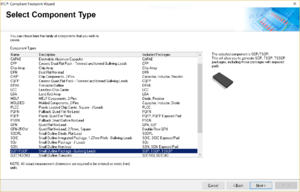
The component you created a symbol for above may already have a footprint in a PCB library; search for it before starting work in this section, and if it exists, skip to "Finishing a Component".
If your component is a standard package, there's a good chance you'll be able to generate your footprint using Altium's IPC Compliant Footprint Generator. Open up the tool ![]() t → i
t → i
Finishing a Component
Pairing Schematic Symbols and Footprints
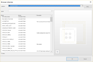
After finishing a schematic symbol and footprint, switch to the schematic symbol in the schematic library editor. In the "Editor" pane at the bottom of the screen, click "Add Footprint," then "Browse." From there, find the relevant PCB footprint library in the dropdown, and then the relevant footprint within the library. Double click the footprint to return to the "Add Footprint" dialogue, where the selected footprint's details will now be shown.
Click "Pin Map," and confirm that the pins on the schematic symbol match up appropriately with the pads on the footprint (if pins were given designators that correspond with their pad numbers, this should have happened automatically). If they don't match, edit the fields until they do. Multiple schematic pins can map to the same footprint pad, but not the other way around - for two pads to connect to the same pin, they must be given the same number in the PCB library editor.
Next, click OK. Your schematic symbol is now paired with a footprint! The footprint should now show up in the list of footprints at the bottom of the Editor pane.
Adding Supplier Links
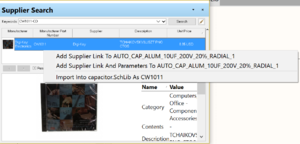
The final step is to add a link to a supplier part, to allow for automated BOM ordering. Open the "Supplier Search" pane ![]() v → w → s → u
v → w → s → u![]() v → w → c → b
v → w → c → b
You're done creating this component! Save the schematic library, and proceed to the final steps below.
Recompiling and SVN Management
Commit Files to SVN
![]() This Altium-related article is a stub. You can help SSI by expanding it.
This Altium-related article is a stub. You can help SSI by expanding it.
